The Jetson AGX / TX2 Camera Interface is the best way to connect MIPI CSI-2 cameras to your NVIDIA TX2 or AGX development system. It handles a wide variety of use cases, provides powerful FPGA-based frame triggering, and uses industry-standard flex cables for camera interconnect.
Key Features
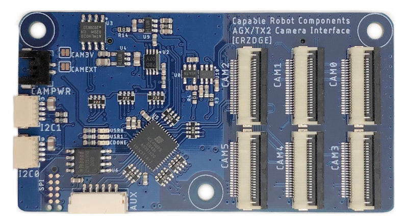
- Designed to install onto NVIDIA AGX and TX2 Development Kit Carriers, as well as any third party carrier which uses the NVIDIA-specified camera interface pinout.
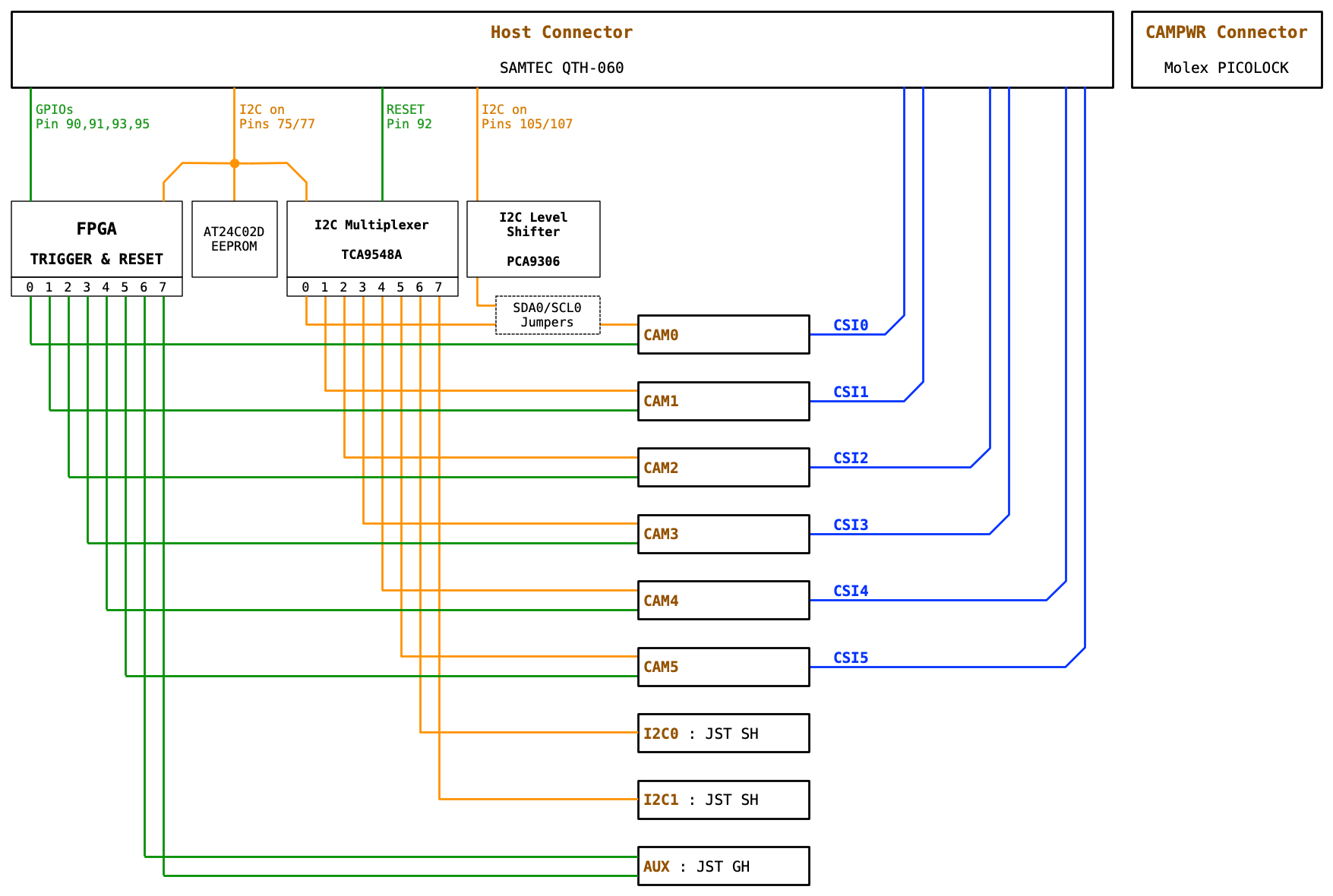
- Exposes 6x MIPI CSI-2 Camera Interfaces (2-lane) on 22-pin, 0.5mm pitch ribbon cable connectors.
- On-board Lattice ICE40UP5K FPGA provides independent or synchronized camera trigger and reset sigals. See section below for Trigger Details.
- Auxiliary Connector (6-pin JST GH) exposes additional 4 GPIO / sync / trigger signals from the FPGA.
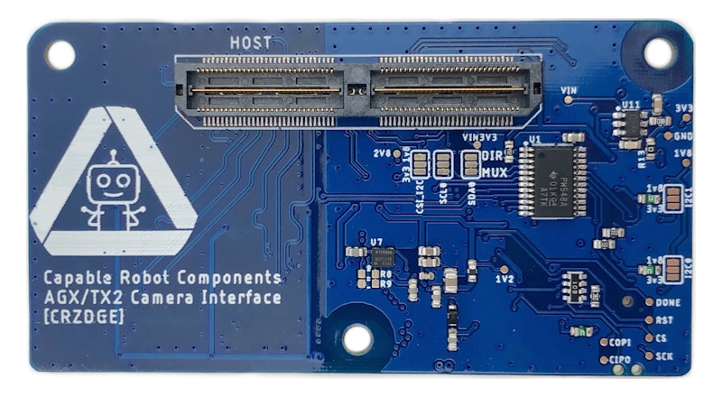
- Camera logic power can be supplied via the Host (3.3v) or 1.8v thru 12v via a 2-pin Molex PICOLOCK connector. The FPGA controls downstream camera logic power via a single high-side switch IC.
- On-board PCA9548A I2C level-shifter and bus isolator allows duplicate I2C devices (imagers, EEPROM, IMU, etc) on each downstream ribbon cable.
- Solder jumpers allow Camera’s 0 I2C bus to be changed from routing through the PCA9548A to a direct connection to the TX2/AGX “general purpose” I2C bus. This allows host-side software higher bandwidth to camera 0 (great for streaming IMU data) while cameras 1 through 5 share use of the host’s “camera” I2C bus.
- PCA9548A bus 6 and 7 are exposed on Sparkfun Qwiic connectors for easy connection to external I2C devices. Solder jumpers allow for 3.3v or 1.8v power to be provided to each JST SH connector.
Volume pricing discounts are available, please contact Capable Robot for details.
FPGA-Based Camera Triggering
The FPGA provides a number of different triggering modes and all triggers are effected by a configurable trigger mask register. CAM0 is bit 0, CAM1 is bit 1, etc. A bit must be set for that output to follow the active trigger.
- Stop: Any active trigger (interval, oneshot, constant, round-robin, or follower) is immediately ended.
- Interval: Repetitious trigger with a specified interval and duration. Trigger duration (length of the trigger pulse) is configuratble from between 1 ms to 255 ms and trigger interval (time between the start of one trigger pulse and the next one) is configurable from between 1 ms and 255 ms.
- Oneshot: A single trigger pulse of between 1 ms and 255 ms is emitted.
- Constant: Triggers go high and stay high.
- Round-Robin: Repetitious triggering like interval, but each trigger pulse is only emitted on a single camera. The next trigger emits on the next sucessive camera (following the active mask), and so on.
- Follower: Auxiliary input 0 or 1 can be selected as the trigger source. Active trigger outputs follow the state of the selected input. This allows one TX2 or AGX host to control the triggering of cameras connected to a seconds TX2 or AGX host.
Open FPGA Gateware
Not only is the FPGA-based triggering gateware powerful and flexible, it is open source and is built using an open-source iCE40 FPGA toolchain.
The gateware is written in nMigen, an open-source toolchain for developing hardware based on synchronous digital logic using the Python programming language. nMigen aims to be easy to learn and use, reduce or eliminate common coding mistakes, and simplify the design of complex hardware with reusable components.
I2C Multiplexing and Level Shifting
The I2C level-shifter / multiplexer and configurable jumpers allow for connection of external I2C sensors and devices, for different I2C voltages to be used for cameras and those external I2C devices, and direct or multiplexed connection to Camera 0.
Resources
These block diagrams are also available as a PDF document.
Data Interconnection
Power Interconnection
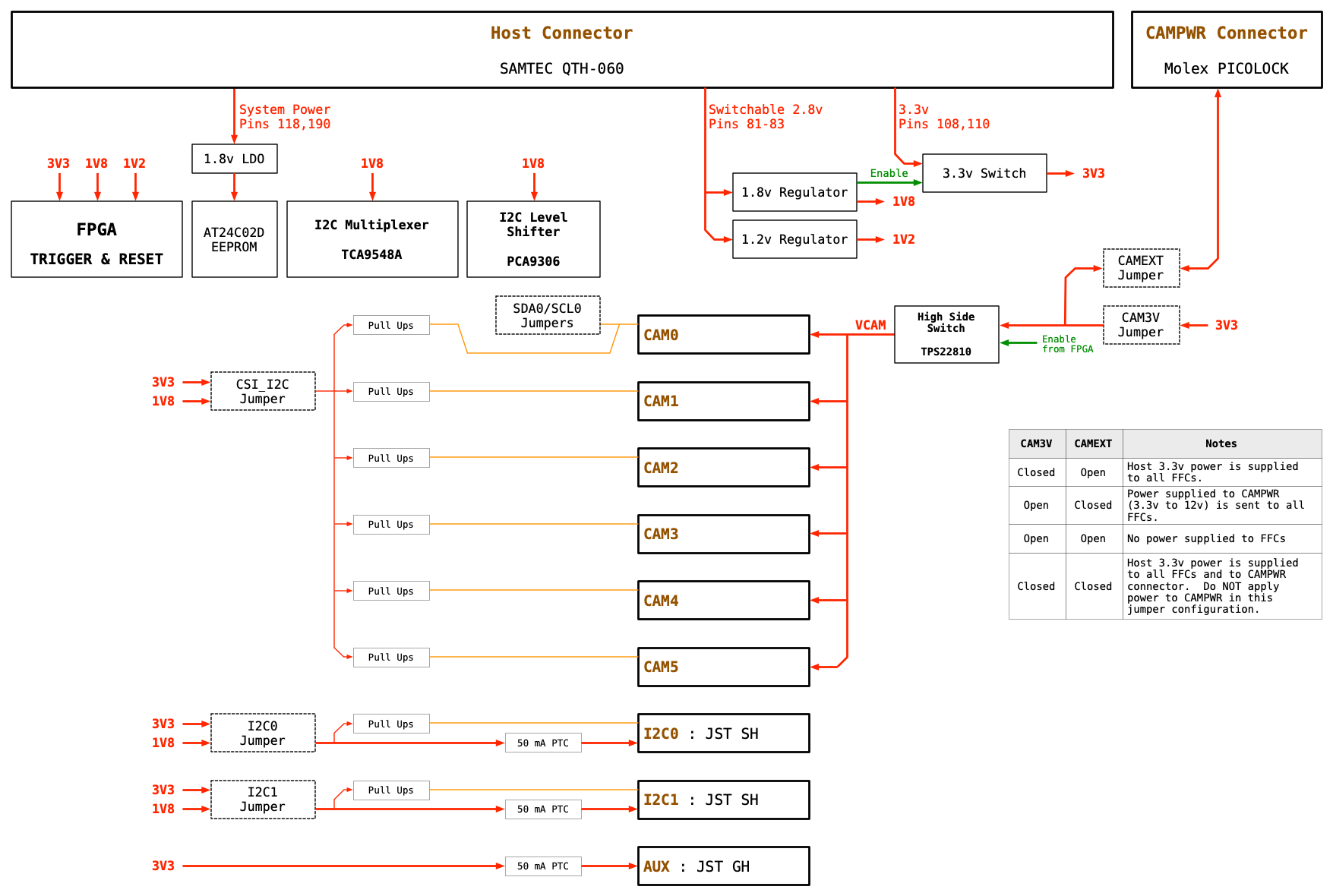
Jumper Settings
| Name | Options | Description |
| I2C0 | 3v3 / 1v8 | Selects the voltage of the I2C0 connector and its' I2C bus. |
| I2C1 | 3v3 / 1v8 | Selects the voltage of the I2C1 connector and its' I2C bus. |
| CSI_I2C | 3v3 / 1v8 | Selects the voltage of all the Camera I2C buses. |
| SDA0 & SCL0 | MUX / DIR | Selects if the CAM0 I2C bus routes through the mux to the host 'camera' I2C bus (as all the other cameras do) or directly to the host 'general purpose' I2C bus. |
| CAM3V | [closed] | When closed, 3.3v provided by the host is used for VCAM (camera logic power on the FFCs). |
| CAMEXT | [open] | When closed, voltage provided to the CAMPWR connector is used for VCAM (camera logic power on the FFCs). If CAMEXT and CAM3V are both closed, 3.3v provided by the host will be present on the CAMPWR connector (as an output) and external voltage SHOULD NOT be applied to the connector. |
Auxiliary IO Connector Pinout
PCB has a 6-pin JST GH connector. Mating connector is GHR-06V-S, pre-crimped leads AGHGH28K305.
| Number | Type | Name | Notes |
| 1 | Power | GND | |
| 2 | Power | 3.3V | Protected via 50mA PTC |
| 3 | GPIO | AUX0 | Controlled by FPGA trigger state && mask bit 6 |
| 4 | GPIO | AUX1 | Controlled by FPGA trigger state && mask bit 7 |
| 5 | GPIO | AUX2 | Controlled by FPGA reset bit 6 |
| 6 | GPIO | AUX3 | Controlled by FPGA reset bit 7 |
Camera Flat-Flex Connector (FFC) Pinouts
The PCB has 6x Wurth 687122149022 connectors : 22-pin, 0.5mm pitch which following the 22-pin Raspberry PI standard. The standard provides for 4-lane MIPI CSI-2 connection, but due to limitations of the TX2 only 2-lane connections are provided on this PCB.
CAM0 connects to the hosts’ CSI0 bus, CAM1 to CSI1, etc.
| Number | Type | Name | Notes |
| 1 | Power | VCAM | Camera logic power provided by host or power input connector (depending on jumper settings) |
| 2 | I2C | SDA | Camera I2C buses have 2.2k pull-ups to 3.3v or 1.8v (selectable via CSI_I2C jumper) |
| 3 | I2C | SCL | Camera I2C buses have 2.2k pull-ups to 3.3v or 1.8v (selectable via CSI_I2C jumper) |
| 4 | Power | GND | |
| 5 | GPIO | TRIG | Controlled by FPGA's trigger state && appropriate bit of trigger mask register |
| 6 | GPIO | RST | Controlled by the appropriate bit of reset register |
| 7 | Power | GND | |
| 8 | Not connected | ||
| 9 | Not connected | ||
| 10 | Power | GND | |
| 11 | Not connected | ||
| 12 | Not connected | ||
| 13 | Power | GND | |
| 14 | CSI | CLK+ | |
| 15 | CSI | CLK- | |
| 16 | Power | GND | |
| 17 | CSI | DATA1+ | |
| 18 | CSI | DATA1- | |
| 19 | Power | GND | |
| 20 | CSI | DATA2+ | |
| 21 | CSI | DATA2- | |
| 22 | Power | GND |